

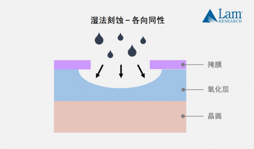
Important considerations in digital IC design
As we all know, the topic of chip design and manufacturing is still occupying people's dinner and dinner time, and the enemy's encircling us makes us discard illusions and rise up to fight. In our work or life, whether we are in the upstream or downstream of the semiconductor industry, we can't avoid the chip, without it, we can't do anything.
When you turn on the air conditioner at home, take out a bottle of cold Coke from the refrigerator, Ge you lay down holding the phone to watch the video, you want the video smooth without any trouble. Behind this, there are groups of chip design engineers, mobile communication engineers, network engineers, image processing engineers, chip development/verification engineers, chip manufacturing engineers, chip packaging and testing engineers... The result of days and nights of hard work.
The design of any chip requires the close cooperation of a large design and verification team. In chip design, we need to consider many factors. So what's going on in our heads?
The chip logic development engineer has three states: circuit in mind, timing in mind, code in hand.
If we are using synchronous design or any IP in our design, or finalizing architecture and microarchitecture, then we need to develop various strategies. Some of them are listed below:
Design for functionality and compatibility
Parallelism, concurrency, and pipelining strategies
External IO and high-speed interfaces
Design area and initial gate number estimates
Speed and maximum frequency requirements
Power requirements and use of low power design
Clock network and latency
Interface and IO latency and modeling strategies
As a result of these considerations, a team of experienced technicians finalized the architecture and microarchitecture of the ASIC/SOC design.
In order to understand the architecture and project development, we need to consider some design factors, mainly in the following areas.
01
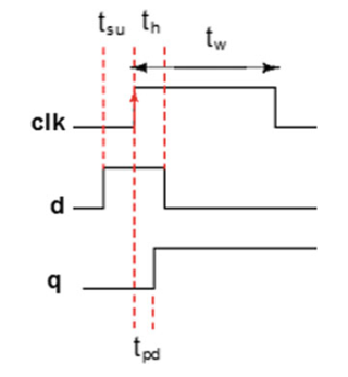
Timing parameter
The important timing parameters of the rising edge sensitive trigger are shown in Figure 1. They are:
Set up time (tsu)
Holding time (th)
Trigger propagation delay (tpd)
Figure 1 D trigger timing parameters
Build time (tsu) : The minimum time for which the data input of the trigger should remain stable until the effective edge of the clock is reached is called the build time.
An effective edge represents the jump from low level to high level of a rising edge (positive edge) sensitive D-flip-flop, and the jump from high level to low level of a falling edge (negative edge) sensitive D-flip-flop.
During the build time window, if the data input goes from 1 to 0 or vice versa, then the trigger output will be metastable, indicating a build violation.
Hold time (th) : The minimum time for the data input of the flip-flop to remain stable after the effective edge of the clock is reached, called the hold time.
An effective edge represents the jump from low to high of a sensitive D flip-flop with a rising edge (positive edge) and from high to low of a sensitive D flip-flop with a falling edge (negative edge).
During the hold time window, if the data input goes from 1 to 0 or vice versa, then the trigger output will be metastable, indicating a hold violation.
Propagation delay of flip-flop (tpd = tcq) : The time required by the flip-flop to produce an effective output after it reaches the effective edge of the clock is called the propagation delay of the flip-flop.
Propagation delay is also known as clock to q terminal delay, also known as tcq.


 快发智造
快发智造

