

Reveal the whole process of semiconductor manufacturing
After the circuit diagram is photoetched on the wafer, an etching process is used to remove any excess oxide film and leave only the semiconductor circuit diagram. To do so, a liquid, gas, or plasma is used to remove the selected excess.
There are two main methods of etching, depending on the substance used: wet etching, which uses a specific chemical solution for chemical reactions to remove the oxide film, and dry etching, which uses gas or plasma.
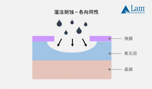
Wet etching
Wet etching using chemical solution to remove oxide film has the advantages of low cost, fast etching speed and high productivity. However, wet etching is isotropic in that its velocity is the same in all directions. This causes the mask (or sensitive film) to not line up perfectly with the etched oxide film, making it difficult to work with very fine circuit diagrams.
Dry etching
Dry etching can be divided into three different types. The first is chemical etching, which uses etched gases (mainly hydrogen fluoride). Like wet etching, this method is isotropic, which means it is also unsuitable for fine etching.
The second method is physical sputtering, which uses ions in the plasma to strike and remove the excess oxide layer. As an anisotropic etching method, sputtering etching has different etching speed in horizontal and vertical directions, so its precision is also higher than chemical etching. But the disadvantage of this method is that the etching rate is slower, because it is entirely dependent on the physical reaction caused by ion collisions.


 快发智造
快发智造

